Schematic gt i9300 s4 pcb galaxy s5 samsung i9500 S5 schematics g903f S5 online galaxy ppt samsung s5 schematic diagram
Samsung Schematic Diagram Free - clipsprogs
Samsung galaxy s5 service schematics Schematic samsung s8 & s8+ (world's first) Tv diagram lg samsung schematic led circuit lcd repair board schematics tips crt v3 interconnect wiring diagrams schema television collection
Schematic diagrams samsung galaxy s5 sm g900f
Samsung schematics and diagramsSamsung s5 galaxy sm schematic g900 diagrams g900f schematics Introducing samsung galaxy s5Schematics galaxy samsung.
Gt-i9500 galaxy s4 pcb schematicSchematic samsung s5 sm galaxy g900f Samsung schematic diagram freeS5 samsung teardown chipworks zerlegt biosensor 16mp fingerprint sensor.
![SAMSUNG SCHEMATICS AND DIAGRAMS - YouTube](https://i.ytimg.com/vi/QfhRtpv_Q8w/maxresdefault.jpg)
[get 29+] galaxy s6 schematic diagram download
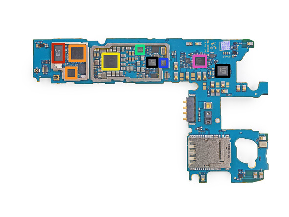
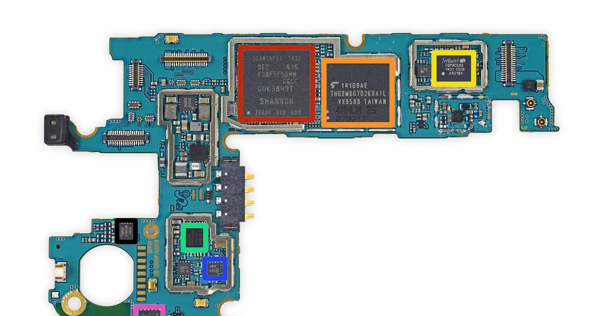
Galaxy samsung s5 schematics service schematic g900Samsung s4 galaxy i9192 mini schematics manual s5 service Galaxy s schematicsSamsung galaxy pcb board components 4g motherboard ic layout solution bluetooth gsm back broadcom wi fi.
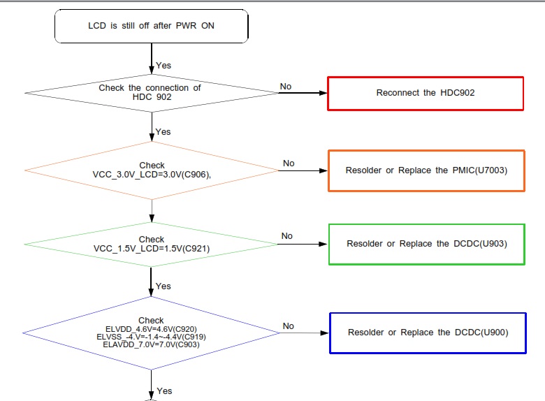
All gsm solution: samsung galaxy s 4g back pcb motherboard ic componentsSamsung schematic diagram schematics diagrams Galaxy s5 h/w. repair guideSchematic diagrams samsung galaxy s5 sm g900f.
![Galaxy S5 H/W. Repair guide - online presentation](https://i2.wp.com/cf.ppt-online.org/files/slide/e/eCIa7jBTMxlYEiOW0sUZNm85HcQXr1FbVoqkD9/slide-40.jpg)
Samsung s5 galaxy schematic g900f g900 schematics service sm technicians
S8 schematic g950f vietfones galaxy mobile1tech vì phát một triểnSamsung galaxy s4 parts diagram Samsung galaxy s5 neo sm-g903f schematicsSamsung galaxy s5 teardown: galaxy s5 hardware components bill at $256.
Galaxy s schematicsSamsung galaxy s5 service schematics .
![Samsung Galaxy S5 Service Schematics](https://i2.wp.com/phonelumi.com/wp-content/uploads/2016/01/samsung-galaxy-s5-schema.jpg)
![Galaxy S Schematics - Cell Schematics & Service Manual PDF](https://i2.wp.com/image.jimcdn.com/app/cms/image/transf/dimension=820x10000:format=jpg/path/s9561acb0f0916d6e/image/ib06629a591b006a4/version/1552166124/samsung-galaxy-s4-i9192.jpg)
![All Gsm Solution: Samsung Galaxy S 4G Back PCB Motherboard IC Components](https://i2.wp.com/lh3.googleusercontent.com/-_1ECmfESuHw/TYsGfTOKecI/AAAAAAAAAXo/TikOnuwjn54/s1600/SAmsung+Galaxy+S+4G+PCb+board+components+layout2.jpg)
![Samsung Galaxy S5 Service Schematics](https://3.bp.blogspot.com/-BdWLNn0D4MY/VdlarifzaWI/AAAAAAAAGO4/O3uIg1MbxBI/s1600/samsung%2Bgalaxy%2Bs5%2Bschematic.jpg)
![Schematic SAMSUNG S8 & S8+ (WORLD'S FIRST) | VietFones Forum](https://i2.wp.com/s1.vietfones.vn/2017/08/99844_947748f07ba6cf9c8374d6f6873e31b0.jpg)
![Samsung Schematic Diagram Free - clipsprogs](https://i2.wp.com/lcdrepairguide.com/V3/images/LG 47LE8500 LED TV Interconnect Diagram.jpg)
![Schematic Diagrams Samsung Galaxy S5 SM G900F - Mobite](https://3.bp.blogspot.com/-v1W090JqE8k/WIZwg4GOdjI/AAAAAAAABZc/wqICEJ-mYswgBRdQUhTk_VwFJbgxiJ7vACEw/s640/OK2NgP5MgJNlMEuJ.jpg)
![Introducing SAMSUNG Galaxy S5](https://i2.wp.com/image.slidesharecdn.com/samsunggalaxys5-140414095228-phpapp02/95/introducing-samsung-galaxy-s5-28-638.jpg?cb=1397469221)
![Samsung Galaxy S5 Teardown: Galaxy S5 Hardware Components Bill at $256](https://i2.wp.com/cdn.wccftech.com/wp-content/uploads/2014/04/Galaxy-S5-Main-Board.jpg)
![Schematic Diagrams Samsung Galaxy S5 SM G900F - Mobite](https://4.bp.blogspot.com/-lr7vOepjt5M/WIZwhmoY4dI/AAAAAAAABZg/EY0kQB29d-YPK9lET2kU_kJLG9Dvn3N-gCLcB/w1200-h630-p-k-no-nu/6VkxB3cCeLRCotVh.jpg)